Vapor Deposition (VD) is a critical thin-film fabrication technology widely applied in semiconductor manufacturing, electronics, aerospace, and other high-tech industries. It involves converting a raw material into a vapor state and then depositing this vapor onto a substrate surface to form a thin film with specific functional properties. Based on distinct deposition mechanisms, vapor deposition is primarily categorized into two major types: Physical Vapor Deposition (PVD) and Chemical Vapor Deposition (CVD). Detailed classifications and characteristics are as follows:
Physical Vapor Deposition (PVD)
Physical Vapor Deposition (PVD) refers to a thin-film deposition process that converts target materials into vapor-phase atoms, molecules, or ions through physical means (e.g., evaporation, sputtering) under vacuum conditions. The vaporized particles then migrate to and deposit on the substrate surface to form a thin film, with no chemical reactions involved in the entire deposition process.
1.1 Main Subtypes
– Vacuum Evaporation Deposition
– Sputter Deposition (e.g., magnetron sputtering, ion beam sputtering)
– Ion Plating Deposition
– Molecular Beam Epitaxy (MBE): A high-precision PVD subtype with ultra-high vacuum requirements
1.2 Core Characteristics
– Operating Environment: Typically conducted under high vacuum conditions (10⁻³ ~ 10⁻⁸ Pa); for MBE, ultra-high vacuum (10⁻⁹ ~ 10⁻¹¹ Pa) is required. High vacuum reduces collisions between vapor particles and air molecules, thereby enhancing thin-film purity.
– Deposition Mechanism: Vapor generation relies on physical processes such as thermal evaporation or ion sputtering, without chemical decomposition or reaction of the target material.
– Film Purity: The prepared thin film features high purity, consistent with the composition of the target material, making it ideal for applications requiring strict composition control.
– Substrate Temperature: Relatively low substrate temperature (usually room temperature to 600°C), avoiding thermal damage to heat-sensitive substrates such as polymers, semiconductors, and delicate electronic components.
– Film Adhesion: Moderate adhesion between the film and substrate; ion plating can significantly improve adhesion by pre-bombarding the substrate with high-energy ions to clean and activate the surface.
– Applicable Materials: Broad material compatibility, including metals, alloys, ceramics, oxides, nitrides, and some organic materials.
Chemical Vapor Deposition (CVD)
Chemical Vapor Deposition (CVD) is a process where gaseous reactants (precursors) are introduced into a reaction chamber. Under controlled conditions (temperature, pressure, gas flow rate), chemical reactions (e.g., decomposition, oxidation, reduction, hydrolysis) occur either on the substrate surface (surface reaction) or in the gas phase (gas-phase reaction). These reactions generate solid products that deposit on the substrate to form a thin film.
2.1 Main Subtypes
– Atmospheric Pressure Chemical Vapor Deposition (APCVD): Operates at normal atmospheric pressure, suitable for large-area deposition.
– Low Pressure Chemical Vapor Deposition (LPCVD): Conducted under low pressure (10⁻¹ ~ 10² Pa), improving film uniformity and step coverage.
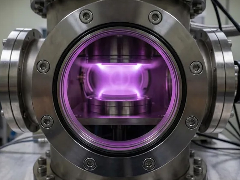
– Plasma Enhanced Chemical Vapor Deposition (PECVD): Uses plasma to activate chemical reactions, reducing reaction temperature.
– Metal Organic Chemical Vapor Deposition (MOCVD): Adopts metal organic compounds as precursors, suitable for depositing compound semiconductor films (e.g., GaN, InP).
2.2 Core Characteristics
– Operating Environment: Versatile operating pressures (atmospheric, low pressure, or plasma-enhanced); low-pressure and plasma conditions effectively enhance film uniformity and reduce reaction temperature.
– Deposition Mechanism: Depends on chemical reactions between gaseous precursors; film composition can be precisely adjusted by modifying precursor types and mixing ratios.
– Film Uniformity: Excellent step coverage and thickness uniformity, particularly suitable for depositing films on substrates with complex shapes, micro-nano structures, or deep trenches (e.g., semiconductor chips, microelectromechanical systems).
– Substrate Temperature: Generally requires higher temperatures (500 ~ 1200°C); PECVD lowers the reaction temperature to 200 ~ 500°C via plasma activation, expanding substrate compatibility.
– Film Adhesion: Strong film-substrate adhesion due to chemical bonding formed at the interface during reaction, ensuring long-term structural stability.
– Applicable Materials: Suitable for preparing various inorganic thin films (oxides, nitrides, carbides, silicides, metal films) and compound semiconductors, widely used in fabricating functional films for semiconductors and electronic devices.
Key Differences Between PVD and CVD
– Deposition Mechanism: PVD relies on physical processes (no chemical reactions); CVD is driven by chemical reactions of gaseous precursors.
– Substrate Temperature: PVD operates at lower temperatures (room temperature ~ 600°C); CVD typically requires higher temperatures (500 ~ 1200°C), except for PECVD (200 ~ 500°C).
– Step Coverage: CVD offers superior step coverage for complex-shaped substrates; PVD is more suitable for flat or simple-structured substrates (MBE excluded, which achieves high precision on planar substrates).
– Film Purity: PVD films have higher purity (consistent with target composition); CVD may introduce trace impurities due to incomplete precursor reactions or by-products.
– Application Scenarios: PVD is widely used for decorative coatings, hard wear-resistant coatings (e.g., TiN), metal conductive films, and high-precision epitaxial films (via MBE); CVD is primarily applied in semiconductor functional films (e.g., gate dielectrics, interlayer dielectrics), high-temperature resistant coatings, and compound semiconductor films.