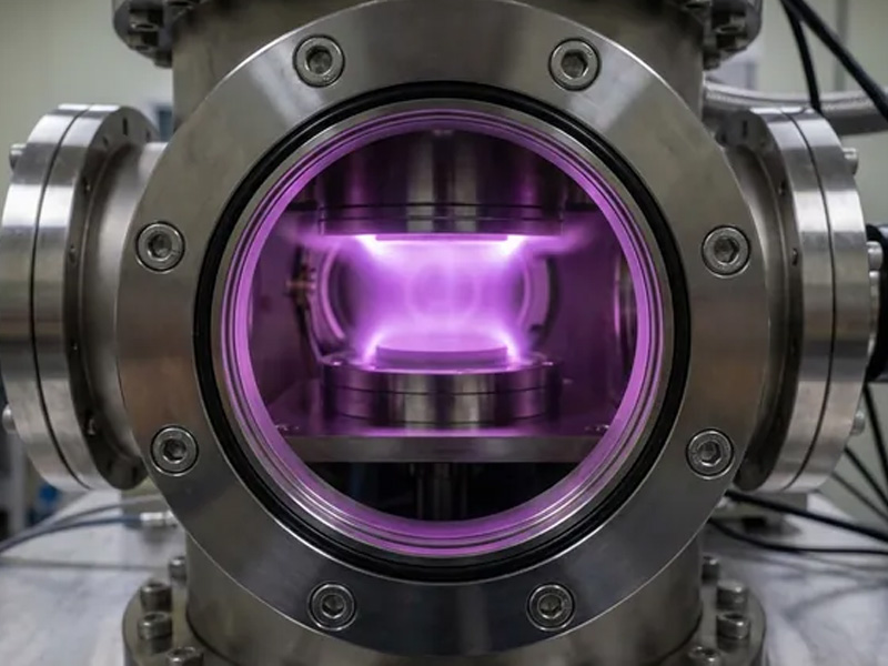
Physical Vapor Deposition (PVD) has emerged as a cornerstone technology in advanced manufacturing, revolutionizing the performance and durability of components across industries such as aerospace, automotive, semiconductor, and medical devices. As a family of vacuum-based coating processes, PVD enables the deposition of thin, high-quality films on various substrates, enhancing properties like wear resistance, corrosion protection, hardness, and biocompatibility. Unlike traditional coating methods, PVD offers superior control over film composition, thickness, and uniformity, making it indispensable for meeting the stringent requirements of modern high-tech applications.
An Overview of PVD: Principles and Core Advantages
At its core, PVD involves the vaporization of a solid material (target) in a high-vacuum environment, followed by the transport of the vaporized particles to a substrate, where they condense to form a thin film. This vacuum-based approach minimizes contamination, ensuring the purity and integrity of the deposited coating. The versatility of PVD lies in its ability to process a wide range of materials, including metals, ceramics, alloys, and composites, adapting to diverse industrial needs. Key advantages of PVD coatings include exceptional adhesion to substrates, high hardness and wear resistance, excellent chemical stability, and precise thickness control—attributes that translate to extended component lifespan, reduced maintenance costs, and enhanced product performance in extreme operating conditions.
Key PVD Techniques: Mechanisms, Advantages, and Applications
Under the PVD umbrella, several distinct techniques have been developed, each tailored to specific material requirements and application scenarios. These techniques differ primarily in how they vaporize the target material, leading to unique film properties and performance characteristics.
Sputter Deposition (Sputtering): The Versatile Workhorse of PVD
Sputter deposition, commonly referred to as sputtering, is one of the most widely adopted PVD methods in industrial production. Its working principle revolves around the use of a glow plasma discharge—often confined around the target material using a magnetic field—to bombard the target surface. The high-energy plasma particles dislodge (sputter) atoms from the target, which then travel through the vacuum and deposit onto the substrate to form a thin film.
The primary advantage of sputtering lies in its versatility: it can deposit a broad spectrum of materials, from metals (e.g., titanium, aluminum) and alloys to ceramics and dielectrics. Additionally, sputtering offers exceptional control over film thickness and uniformity, making it ideal for applications requiring consistent coating quality across large or complex-shaped substrates. Common industrial applications include semiconductor wafer metallization, decorative coatings for consumer electronics, wear-resistant coatings for automotive engine components, and corrosion protection for aerospace parts.
Evaporative Deposition (Thermal Evaporation): Efficient Coating for High-Melting-Point Materials
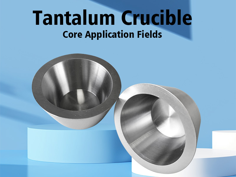
Evaporative deposition, or thermal evaporation, relies on heating the target material to a high vapor pressure in a high-vacuum environment. This heating is typically achieved via electrical resistance heating (for low-melting-point materials) or electron beam bombardment (for high-melting-point materials like tungsten, tantalum, or ceramics). Once vaporized, the material particles condense on the cooler substrate surface, forming a thin film.
Electron-beam PVD (EB-PVD), a specialized form of thermal evaporation, is particularly renowned for its ability to process high-melting-point materials—an advantage that makes it critical for aerospace applications, such as coating turbine blades with thermal barrier coatings (TBCs) to withstand extreme temperatures. Evaporative deposition is also valued for its high deposition rate and simplicity, making it suitable for high-volume production of optical coatings (e.g., anti-reflective coatings for lenses) and thin-film metallization in electronic devices.
Cathodic Arc Deposition (Arc PVD): High-Density Coatings for Extreme Wear Resistance
Cathodic arc deposition, or Arc PVD, employs a high-power electric arc discharged directly at the target material. The intense heat and energy of the arc “blasts” away portions of the target, converting it into a highly ionized vapor. This ionized vapor is then accelerated toward the substrate, where it deposits to form a dense, adherent thin film.
The defining feature of Arc PVD is its ability to produce coatings with exceptional density and adhesion—properties that make them ideal for applications requiring extreme wear and corrosion resistance. Arc PVD coatings are widely used in the automotive industry (e.g., coating cutting tools, gears, and piston rings), as well as in the manufacturing of molds and dies for plastic and metal forming. Additionally, the high ionization level of the vapor allows for precise control over film structure, enabling the deposition of advanced composite coatings tailored to specific performance requirements.
Pulsed Laser Deposition (PLD): Precision Coating for Complex Materials
Pulsed Laser Deposition (PLD) utilizes a high-power pulsed laser to ablate (vaporize) material from the target surface, creating a plasma plume of vaporized particles. This plume travels through the vacuum and deposits onto the substrate, forming a thin film. Unlike other PVD techniques, PLD offers unparalleled control over film stoichiometry—the precise ratio of elements in the coating—making it uniquely suited for depositing complex materials such as oxides, nitrides, and multi-component alloys.
PLD’s precision makes it a preferred choice for advanced research and high-tech applications, including the development of superconducting films, ferroelectric coatings for electronic devices, and biocompatible coatings for medical implants (e.g., orthopedic implants and dental tools). While PLD is often used in laboratory and low-volume production settings, advancements in laser technology are expanding its adoption in industrial-scale manufacturing of high-value components.
The Future of PVD: Innovations Driving Industry Advancement
As advanced manufacturing continues to evolve, PVD technology is undergoing continuous innovation to meet increasingly demanding application requirements. Ongoing developments include the integration of PVD with other surface modification techniques (e.g., plasma nitriding) to create multi-layered coatings with enhanced performance, the optimization of vacuum systems for higher deposition rates and lower energy consumption, and the development of PVD processes for emerging materials such as 2D materials and nanocomposites.
For manufacturers, adopting PVD technology is not just a means of enhancing product performance—it is a strategic investment in competitiveness. By leveraging the unique advantages of different PVD techniques, companies can develop high-quality, durable products that excel in extreme environments, while reducing maintenance costs and improving sustainability through extended component lifespans.
Conclusion
PVD technology has established itself as a critical enabler of advanced manufacturing, offering versatile, precise, and high-performance coating solutions across a wide range of industries. From the versatility of sputtering to the precision of PLD, each PVD technique brings unique capabilities that address specific material and application needs. As innovation in PVD continues to accelerate, its role in driving technological advancement—from aerospace and semiconductors to medical devices and automotive—will only grow stronger. For businesses looking to stay at the forefront of their industries, understanding and leveraging PVD technology is essential to unlocking new levels of product performance and operational efficiency.