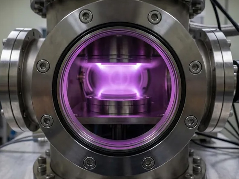
Tantalum ion implantation technology is an advanced material surface modification process. It involves implanting tantalum ions into the substrate surface as a high-energy beam in a vacuum environment, forming a special modified layer on the substrate surface to significantly optimize material performance. Tantalum ion implantation parts manufactured based on this technology, with their unique performance advantages, demonstrate irreplaceable application value in high-end manufacturing fields such as semiconductors, biomedicine, and aerospace.
Excellent Environmental Resistance: Core Support for Adapting to Extreme Working Conditions
Tantalum itself has inherent advantages such as high melting point and strong chemical inertness. After ion implantation modification, the tantalum-rich modified layer formed on the part surface further enhances environmental adaptability, enabling stable performance under extreme working conditions such as high temperature, corrosion, and strong radiation. This is the core foundation for its foothold in high-end manufacturing fields.
Outstanding High-Temperature Resistance and Creep Resistance
Tantalum has a melting point as high as 2996°C, far exceeding that of conventional metal materials such as stainless steel (approximately 1500°C) and aluminum (660°C). After ion implantation, the modified layer on the part surface inherits the high-temperature stability of tantalum, maintaining structural integrity without deformation or failure even in extreme temperature environments ranging from several hundred to several thousand degrees Celsius. This advantage makes it indispensable in core components of semiconductor ion implanters, such as ion source chambers and transport pipelines—these components need to work long-term under the combined action of high temperature and strong electromagnetic fields, and the tantalum ion implantation layer can effectively prevent pipeline creep deformation and ensure the stability of ion beam transmission. Meanwhile, in applications such as high-temperature sensor protection tubes and high-power electron tube anode support structures in the aerospace field, this performance can also ensure the long-term reliable operation of parts in extreme temperature environments.
Superb Chemical Corrosion Resistance
Tantalum exhibits extremely strong chemical inertness to most inorganic acids (except hydrofluoric acid) and high-temperature corrosive gases (such as fluorine-based gases and chlorine-based gases). The modified layer formed after tantalum ion implantation further constructs a dense “corrosion barrier” on the substrate surface. In semiconductor manufacturing processes such as etching and Chemical Vapor Deposition (CVD), the reaction gases are mostly high-temperature and highly corrosive media (such as HF, Cl₂, NF₃, etc.). Tantalum ion implantation parts can withstand long-term erosion by these media, avoiding pipeline dissolution or impurity release that would contaminate wafers, thus ensuring the high-purity requirements of semiconductor manufacturing. Compared with traditional corrosion-resistant materials such as nickel-based alloys and stainless steel, tantalum ion implantation parts have better corrosion resistance in common corrosive environments of semiconductors, and do not react with key semiconductor materials such as silicon, aluminum, and copper, further improving process stability. In addition, in fields with complex corrosive media such as chemical industry and nuclear industry, such parts can also significantly extend service life and reduce maintenance costs.
Excellent Sputtering Resistance and Low Impurity Release Characteristics
Under special working conditions such as ion beam bombardment and plasma scouring, tantalum ion implantation parts have an extremely low sputtering rate—that is, the probability of surface atoms being knocked off is much lower than that of traditional materials. This characteristic is crucial in the semiconductor ion implantation process: the detachment of surface atoms will introduce impurities, affecting wafer doping accuracy (semiconductor manufacturing requires error control at the ppm level). The tantalum ion implantation layer can effectively reduce impurity introduction and ensure doping uniformity and accuracy. At the same time, the substrate of tantalum ion implantation parts is strictly purified, and the purity of the implanted tantalum ions can reach more than 99.95% (even ultra-high purity 99.99%), which itself releases almost no metal impurities (such as iron, nickel, etc.), fully meeting the “zero-defect” manufacturing requirements of semiconductors and the cleanliness requirements of high-end precision instruments.
Precise Performance Regulation: Core Advantage for Adapting to Multi-Scenario Needs
Tantalum ion implantation technology can precisely control the composition, thickness, and structure of the surface modified layer by adjusting parameters such as implantation energy, dose, and time, thereby realizing customized optimization of the part’s surface hardness, wear resistance, biocompatibility, and other properties to adapt to the differentiated needs of different industries.
Customizable Surface Hardness and Wear Resistance
By adjusting tantalum ion implantation parameters, a composite modified layer with high hardness and strong wear resistance can be formed on the substrate surface—tantalum ions interact with substrate atoms through substitution, doping, and other interactions, changing the crystal structure of the substrate surface, and significantly improving the surface hardness and wear resistance compared with the substrate itself. This advantage makes it widely used in wear-resistant components (such as bearings, gears, key friction parts of engines) in fields such as mechanical manufacturing and aerospace: it can effectively reduce component wear rate, extend service life, and reduce cost losses caused by frequent replacement. Compared with traditional surface strengthening processes such as coating and quenching, the modified layer formed by tantalum ion implantation has a tighter combination with the substrate, is not easy to fall off or peel off, and does not significantly change the overall size and mechanical properties of the substrate, making it suitable for surface strengthening of precision parts.
Customized Biocompatibility and Bioactivity
By adjusting the tantalum ion implantation time, modified layers with different components (such as Ta, Ta/Ta₂O₅, Ta/Ta₂O₅₋ₓ/Ta₂O₅) can be constructed on the surface of biomedical materials (such as nitinol), precisely optimizing their biological properties to meet the strict requirements of the biomedical field. For example, tantalum ion implantation on the surface of nitinol vascular stents can significantly improve the blood compatibility of the stents: the number of platelet adhesion on the modified surface is significantly reduced, and the platelets basically maintain an unactivated spherical state, which can effectively reduce the risk of thrombosis; at the same time, the modified layer has good hydrophilicity, can provide more cell adhesion sites, promote the early adhesion, spreading, and proliferation of human umbilical vein endothelial cells, accelerate the repair of damaged vascular intima, and reduce the probability of stent restenosis. In addition, in the field of orthopedic and dental implants, the tantalum ion implantation layer can simulate the microenvironment of human bone tissue, stimulate new bone formation, and improve the integration of implants with bone tissue. At the same time, its elastic modulus can be adjusted close to that of bone tissue through parameter control, reducing the impact of the “stress shielding effect” on bone repair.
Excellent Process Compatibility: Key Guarantee for Promoting High-End Manufacturing Upgrading
Tantalum ion implantation parts not only have excellent performance themselves but also can be perfectly compatible with various high-end manufacturing processes, providing support for industry technology upgrading, and showing unique value especially in high-end fields such as semiconductors, precision electronics, and biomedicine.
Adapting to High-Precision Requirements of Advanced Semiconductor Processes
As semiconductor processes advance to 7nm and below advanced nodes, the requirements for the precision and stability of core components of manufacturing equipment have become increasingly stringent. The low impurity release, high dimensional stability, and excellent corrosion and sputtering resistance of tantalum ion implantation parts exactly match the high-purity and high-precision manufacturing requirements of advanced processes. For example, in ion implanters, their transport pipelines can ensure the stable transmission of high-purity ion beams and improve wafer doping accuracy; in CVD equipment, as reaction gas transport pipelines, they can avoid impurity contamination of thin films and ensure the uniformity and reliability of chip circuit layers. It can be said that tantalum ion implantation parts are one of the important material supports for the breakthrough of advanced semiconductor processes.
Adapting to High Air-Tightness Requirements of Precision Electronics and Vacuum Systems
Tantalum has excellent ductility and can achieve high air-tightness connections through welding or cold working. Tantalum ion implantation parts inherit this characteristic and perform excellently in vacuum systems. In fields such as semiconductor manufacturing and vacuum electronic devices, equipment needs to maintain an extremely high vacuum environment (usually ≤10⁻⁶Pa). Tantalum ion implantation parts can be used as vacuum pipeline connection components to effectively prevent the infiltration of external air (including oxygen and water vapor), avoiding wafer oxidation or vacuum device performance failure. At the same time, in precision electronic components such as electrode lead sleeves of high-voltage tantalum capacitors, the tantalum ion implantation layer can use the dense oxide film (Ta₂O₅) easily formed on the tantalum surface to improve insulation, ensuring the stability and service life of the capacitors.
Adapting to Sterility and Long-Term Implantation Requirements of Biomedicine
Biomedical implants need to meet strict requirements such as sterility, non-toxicity, and long-term implantation stability. The modified layer of tantalum ion implantation parts is dense and uniform, without pores or cracks, which can effectively block the release of harmful ions (such as nickel ions in nitinol) from the substrate and reduce biological toxicity; at the same time, its excellent resistance to body fluid corrosion can ensure that the parts are long-term stable in the human body fluid environment without degradation or performance deterioration. In addition, the tantalum ion implantation process can be carried out in a sterile environment, and no additional impurities will be introduced on the part surface, fully complying with the cleanliness standards of biomedical materials, and providing a reliable material solution for implantable devices in fields such as orthopedics, cardiovascular, and dentistry.
Long-Term Service Life: Core Value Embodiment of Cost Reduction and Efficiency Improvement
By enhancing surface performance, tantalum ion implantation parts fundamentally improve the anti-failure ability of parts under extreme working conditions and complex environments, significantly extending their service life. Compared with traditional unmodified parts or other surface-treated parts, tantalum ion implantation parts do not require frequent replacement, which can effectively reduce equipment maintenance frequency and downtime—this is particularly important in high-end fields such as semiconductor manufacturing, aerospace, and biomedicine: the equipment downtime cost in these fields is extremely high, and the extended service life of parts can directly improve production efficiency and reduce overall costs. For example, the service life of tantalum ion implantation pipelines in semiconductor etching equipment can be 3-5 times that of traditional stainless steel pipelines; tantalum ion implantation vascular stents for biomedicine can be stably implanted in the human body for a long time, reducing the risk of secondary surgery and the medical costs of patients. At the same time, the tantalum ion implantation process has high stability and reliability, with small performance differences between part batches, which can further improve the quality stability of downstream products and reduce the product scrap rate caused by part performance fluctuations.
Conclusion
Tantalum ion implantation parts have established unique competitive advantages in the high-end manufacturing field by virtue of their excellent environmental resistance, precise performance regulation ability, excellent process compatibility, and long-term service life. With the technological upgrading of industries such as semiconductors, biomedicine, and aerospace, the requirements for material performance are constantly improving. The application scenarios of tantalum ion implantation technology will be further expanded, and the core value of tantalum ion implantation parts will become increasingly prominent. In the future, with the optimization of implantation processes and the breakthrough of cost control, such parts are expected to penetrate more mid-end manufacturing fields, promoting material upgrading and quality improvement of the entire manufacturing industry.