Physical Vapor Deposition (PVD) stands as a cornerstone of advanced surface engineering, enabling the fabrication of high-performance thin films that enhance the functional properties of substrates across diverse industrial sectors. Distinguished from Chemical Vapor Deposition (CVD) by its physical material transfer mechanism—avoiding chemical reactions of gaseous precursors—PVD processes involve the conversion of a solid or liquid source material into a vapor phase, followed by condensation onto a target substrate to form a coherent thin film. This atom-by-atom deposition approach yields coatings with exceptional purity, uniformity, and adhesion, making PVD indispensable for applications demanding precise control over surface characteristics such as hardness, wear resistance, corrosion protection, optical transmittance, and electrical conductivity.
Core Fundamentals of PVD Technology
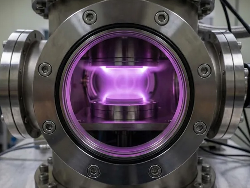
At its essence, PVD relies on three sequential stages: vaporization of the source material, transport of the vapor from the source to the substrate, and condensation of the vapor into a thin film. All stages occur within a high-vacuum environment, which serves two critical purposes: first, it minimizes collisions between vapor particles and atmospheric molecules, ensuring unobstructed transport to the substrate; second, it reduces contamination of the coating, preserving its chemical purity. Unlike CVD, which relies on chemical decomposition or reaction of gaseous precursors, PVD’s physical transfer mechanism enables better control over film composition and thickness, particularly for metallic and ceramic coatings.
Key Components of a PVD System
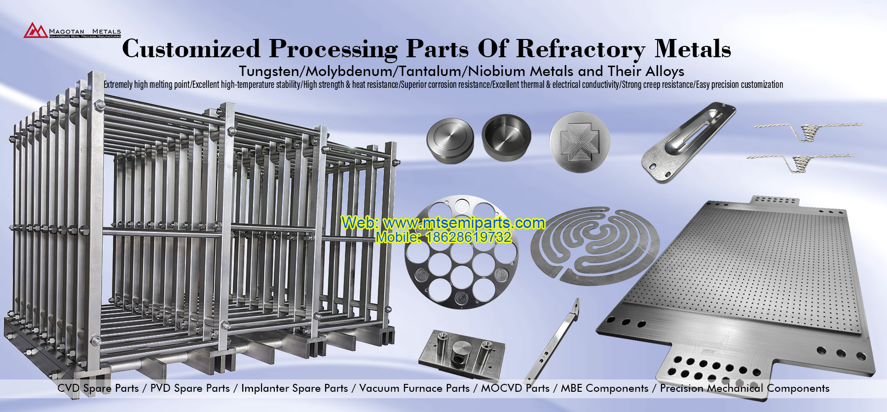
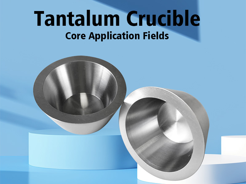
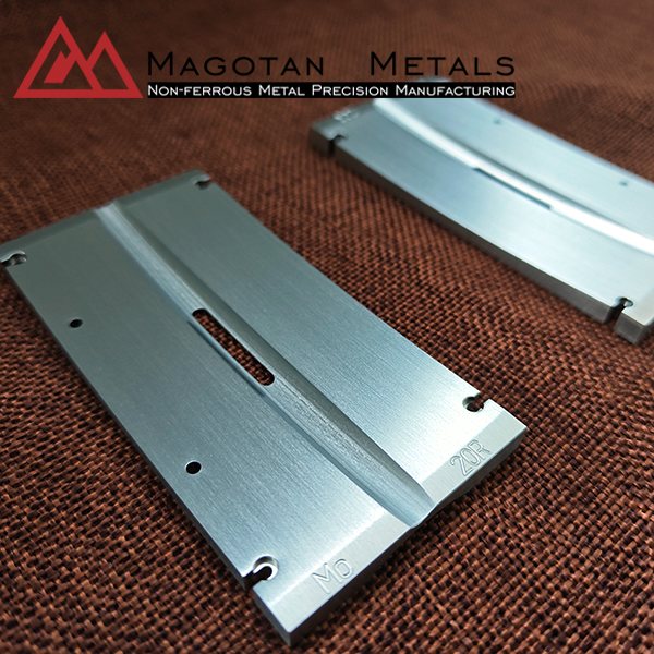
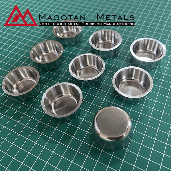
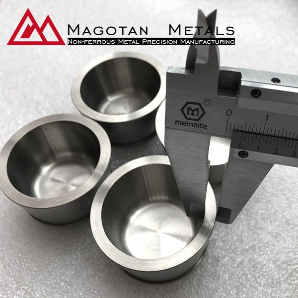
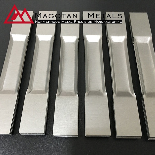
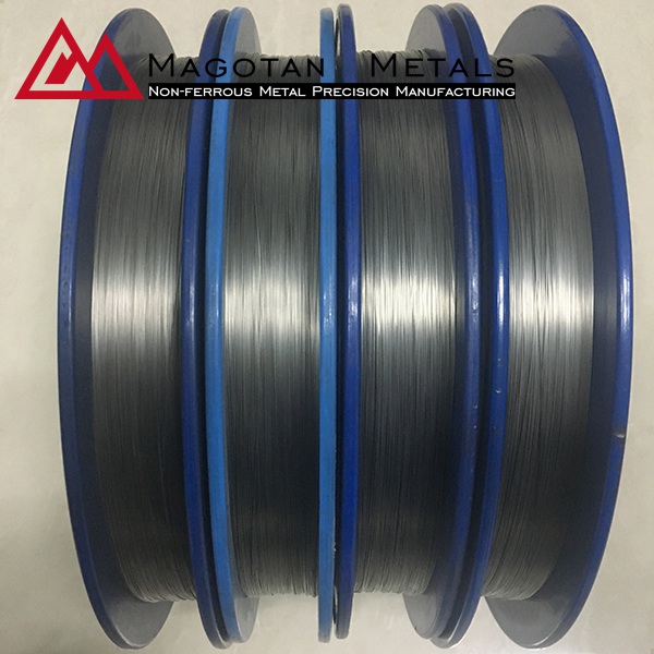
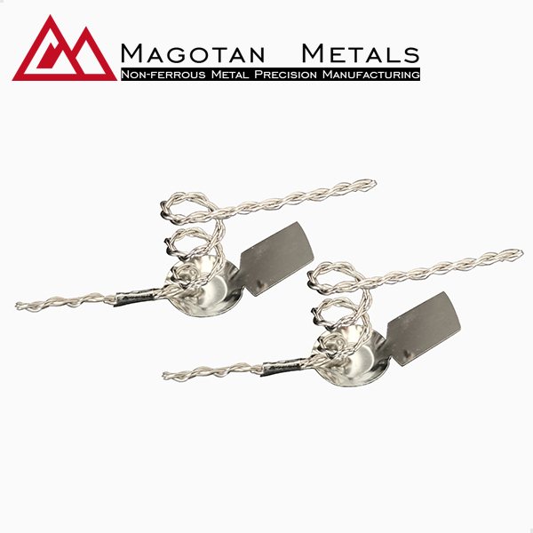
A typical PVD system comprises four essential components: (1) A vacuum chamber, where the deposition process takes place, equipped with pumps to achieve and maintain high vacuum levels (usually 10⁻³ to 10⁻⁸ Torr); (2) A source material (target), which is the material to be deposited as a thin film—among which refractory metal workpieces (e.g., tungsten, molybdenum, tantalum, niobium) are ideal choices for high-demand scenarios due to their ultra-high melting points and excellent thermal stability; (3) A vaporization source, which provides the energy required to convert the target from solid/liquid to vapor (e.g., thermal evaporation heaters, sputtering cathodes, or arc evaporation electrodes); (4) A substrate holder, which secures the target substrate and may include heating or biasing capabilities to optimize film adhesion and structure.
Classification of PVD Processes
PVD processes are primarily categorized based on the vaporization mechanism, with three dominant technologies:
• Thermal Evaporation: The simplest PVD technique, where the source material is heated (via resistance heating, electron beam, or laser) to its vaporization temperature. Vapor particles travel directly to the substrate and condense. Widely used for optical coatings (e.g., anti-reflective coatings on glass) due to its ability to produce uniform, thin films.
• Sputtering: Involves bombarding the source target with high-energy ions (usually argon) to dislodge (sputter) atoms or molecules, which then condense on the substrate. Sputtering offers superior film adhesion and uniformity compared to thermal evaporation, making it ideal for decorative coatings, hard coatings for cutting tools, and thin films for semiconductor devices.
• Arc Evaporation (Cathodic Arc Deposition): Uses an electric arc to melt and vaporize the target material, producing a high-density plasma of the source material. The plasma is then directed toward the substrate, where it condenses into a thin film. This process yields extremely hard and wear-resistant coatings (e.g., TiAlN, CrN) for industrial tooling and automotive components.
Critical Advantages of PVD Coatings
The unique deposition mechanism of PVD imparts several advantages over alternative coating technologies, positioning it as a preferred choice for high-performance applications:
Superior Coating Purity and Uniformity
The high-vacuum environment of PVD systems minimizes contamination from atmospheric gases (e.g., oxygen, nitrogen, moisture), resulting in coatings with high chemical purity. Additionally, precise control over vaporization and transport parameters ensures uniform film thickness across large substrate areas, a critical requirement for optical and electronic applications.
Exceptional Mechanical and Chemical Properties
PVD coatings exhibit excellent adhesion to the substrate, reducing the risk of flaking or delamination under mechanical stress. Many PVD coatings (e.g., titanium nitride, zirconium nitride) are extremely hard (2000–4000 HV) and wear-resistant, extending the service life of components such as cutting tools, dies, and gears. They also provide effective corrosion protection, as the dense film acts as a barrier against moisture, chemicals, and oxidation.
Versatility and Environmental Friendliness
PVD can deposit coatings on a wide range of substrates, including metals, ceramics, glass, polymers, and composites. It supports a broad spectrum of coating materials, from pure metals to alloys and ceramics, enabling customization for specific application requirements. Furthermore, PVD processes are inherently environmentally friendly compared to electroplating (a common alternative), as they do not use toxic electrolytes or generate hazardous waste.
Key Industry Applications of PVD
The versatility and performance of PVD coatings have made them integral to numerous industries, spanning manufacturing, electronics, automotive, aerospace, and optics. Below are the most prominent application areas:
Manufacturing and Tooling
PVD is widely used to coat cutting tools (drills, end mills, inserts), dies, and molds. For machining processes involving high-temperature, high-pressure, or difficult-to-cut materials (e.g., superalloys), coatings deposited usingrefractory metal workpieces as targets (such as tungsten-based or molybdenum-based alloys) exhibit exceptional thermal stability and wear resistance. Compared to conventional TiN, TiAlN coatings, these refractory metal-enhanced coatings further extend tool life by up to 10 times compared to uncoated tools, translating to higher machining speeds, improved surface finish of workpieces, and reduced tool replacement costs.
Electronics and Semiconductors
In the electronics industry, PVD is critical for fabricating thin films for semiconductors, flat-panel displays, and solar cells. For high-power semiconductor devices or components operating in high-temperature environments, refractory metal workpieces (e.g., tantalum, niobium targets) are employed in sputtering processes to deposit high-temperature-resistant conductive films, ensuring stable electrical performance under extreme conditions. Additionally, sputtering is used to deposit conventional conductive films (e.g., aluminum, copper) for interconnects in integrated circuits, as well as transparent conductive oxides (TCOs) such as indium tin oxide (ITO) for touchscreens and displays. Thermal evaporation is employed to deposit metal contacts for solar cells, with refractory metal-based evaporation sources enhancing process stability.
Automotive and Aerospace
Automotive applications of PVD include coating engine components (valves, piston rings), transmission parts, and decorative trim (e.g., chrome-like coatings on wheel rims and interior trim). For high-temperature engine components (such as turbocharger blades), PVD coatings deposited on refractory metal workpieces (e.g., molybdenum-alloyed substrates) enhance wear resistance and thermal fatigue performance, reducing friction to improve fuel efficiency. In aerospace, PVD coatings are even more crucial—turbine blades, landing gear components, and aircraft fasteners often adopt refractory metal workpieces as substrates or target materials for PVD coating, enabling them to withstand extreme temperatures (exceeding 1000°C), corrosion, and mechanical stress in high-altitude flight environments.
Optics and Photonics
PVD is the primary technology for manufacturing optical coatings, such as anti-reflective coatings (AR) on eyeglasses, camera lenses, and solar panels; reflective coatings (e.g., aluminum or silver) on mirrors; and filter coatings for telescopes and optical sensors. Thermal evaporation is preferred for these applications due to its ability to produce ultra-thin, uniform films with precise optical properties.
Emerging Trends and Future Outlook of PVD
As industries demand increasingly advanced materials and performance, PVD technology continues to evolve, with several key trends shaping its future:
Nanostructured and Multilayer PVD Coatings
Research is focused on developing nanostructured PVD coatings (with grain sizes < 100 nm) and multilayer coatings (alternating layers of different materials) to enhance properties such as hardness, toughness, and corrosion resistance. For example, nanostructured TiAlN coatings exhibit higher hardness and thermal stability than conventional TiAlN, making them suitable for high-speed machining of difficult-to-cut materials.
Hybrid PVD-CVD Processes
Hybrid processes that combine PVD and CVD technologies (e.g., Plasma-Enhanced CVD (PECVD) integrated with sputtering) are gaining traction. These hybrid systems leverage the advantages of both technologies, enabling the deposition of complex coatings with tailored properties. For instance, hybrid PVD-CVD processes can produce diamond-like carbon (DLC) coatings with superior hardness and low friction for automotive and medical applications.
Application Expansion in Biomedical and Renewable Energy
PVD is increasingly being adopted in the biomedical industry to coat implants (e.g., hip replacements, dental implants) with biocompatible materials. Refractory metal workpieces (e.g., tantalum, niobium) are particularly suitable for this field due to their excellent biocompatibility, corrosion resistance in human body fluids, and high strength—PVD coatings on these refractory metal implants further improve osseointegration (bone bonding) and reduce the risk of implant rejection. In renewable energy, PVD is used to deposit protective and conductive coatings for wind turbine components (e.g., gearbox parts) and advanced solar cells (e.g., perovskite solar cells). Refractory metal workpieces serve as durable targets for depositing high-temperature-resistant coatings on wind turbine components, enhancing their service life in harsh outdoor environments, while also improving the efficiency and stability of solar cell conductive layers.
Conclusion
Physical Vapor Deposition (PVD) has established itself as a vital technology in advanced surface engineering, driven by its ability to produce high-purity, high-performance thin films with tailored properties. The integration of refractory metal workpieces—leveraging their unique high-temperature stability, strength, and corrosion resistance—has further expanded PVD’s application boundaries in high-demand sectors such as aerospace, high-power electronics, and biomedical engineering. From manufacturing tooling to electronics, automotive, and aerospace, PVD’s versatility combined with the superior properties of refractory metal workpieces makes it indispensable for modern industries. As research advances, the development of nanostructured coatings, hybrid processes, and expansion into emerging sectors like biomedical and renewable energy will further solidify the synergistic role of PVD and refractory metal workpieces as cornerstones of future manufacturing and technology innovation.