Skip image slider
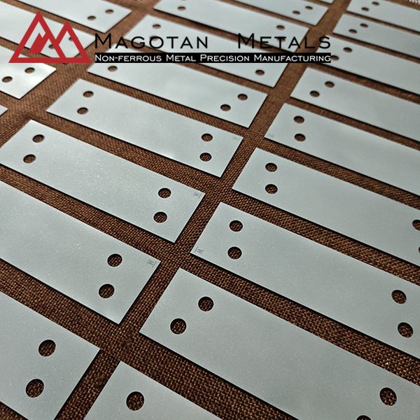
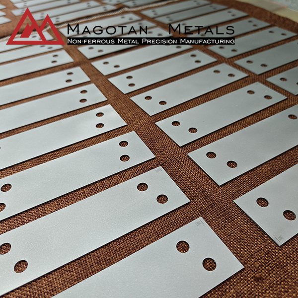
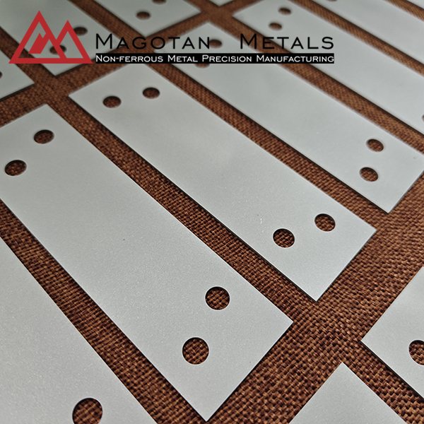
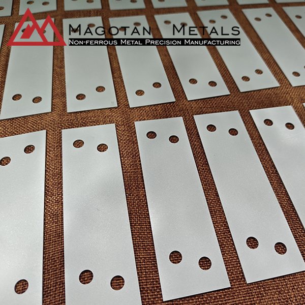
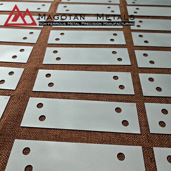

Showing Slide 1 of 6: 99.95% purity tungsten ion implantation components for semiconductor
Tungsten Ion Implantation Components – Ultra-Precision Refractory Parts for Semiconductor Processing
As a professional refractory metal manufacturer, ourTungsten Ion Implantation Components are engineered to meet the rigorous requirements of advanced semiconductor processing, solar cell manufacturing, and research accelerator systems. Crafted from ultra-high-purity tungsten, these components integrate precision machining, extreme environment resistance, and custom adaptation to deliver unparalleled performance and reliability—effectively addressing the pain points of contamination, short service life, and beam instability in ion implantation processes.
-
Ultra-Low Contamination Design: 99.95%+ purity and proprietary surface treatment reduce contamination, ideal forsemiconductor doping tungsten components.
-
Extreme Durability: 3422°C melting point and HV380-420 hardness deliver 3-5X longer life for high-temperature ion beam tungsten parts.
-
Implanter-Specific Customization: ±0.005mm tolerance and OEM designs enable custom tungsten implantation components for major brands.
-
Enhanced Beam Stability: Ra≤0.3μm surface and uniform density ensure precision for precision doping tungsten components.
-
Vacuum Compatibility: Specialized cleaning eliminates outgassing for semiconductor vacuum tungsten parts.
Products Categories
Get A Free Quote
Why Choose Our Tungsten Ion Implantation Components?
Our products outperform standard tungsten components with high-end semiconductor-focused features:
-
Ultra-Low Contamination Design: Boasting 99.95%+ purity and a proprietary surface treatment process, our components minimize particle generation and impurity diffusion—critical for semiconductor doping tungsten components and silicon wafer processing workflows.
-
Extreme Wear & Temperature Endurance: With a melting point of 3422°C and optimized hardness (HV 380-420), they resist prolonged ion bombardment and sustain operating temperatures up to 2500°C, achieving 3-5X longer service life than generic parts—ideal for high-temperature ion beam tungsten parts.
-
Implanter-Specific Customization: We offer precision machining with ±0.005mm tolerances (tighter than industry standard ±0.01mm) and OEM-compatible designs for major implanter brands (Applied Materials, Axcelis, etc.), providing custom tungsten implantation components that fit seamlessly without modification.
-
Beam Stability Enhancement: An ultra-smooth surface (Ra ≤0.3μm, superior to the industry standard of ≤0.4μm) and uniform material density (19.3 g/cm³) ensure consistent ion beam control, reducing beam drift forprecision doping tungsten components.
-
Vacuum-Sealed Compatibility: Specialized cleaning and surface passivation processes eliminate outgassing, making our components suitable for high-vacuum ion implantation systems—perfect for semiconductor vacuum tungsten parts.
Specifications of Tungsten Ion Implantation Components
|
Parameter
|
Value
|
|---|---|
|
Material
|
Pure Tungsten (W) / Tungsten Alloy (Optional)
|
|
Purity
|
≥99.95%
|
|
Density
|
19.3 g/cm³
|
|
Hardness (HV)
|
380-420
|
|
Surface Roughness
|
Ra ≤0.4μm
|
|
Operating Temperature
|
Up to 2500°C (Short-Term: 2800°C)
|
Value to Customers by Our Tungsten Ion Implantation Components
For OEM-grade Tungsten Ion Implantation Components that boost production efficiency and lower maintenance costs, get in touch with our specialists today.
Application Fields
Our Tungsten Ion Implantation Components are indispensable in high-precision manufacturing and research applications:
-
Advanced Semiconductor Manufacturing: Used in 7nm/5nm process silicon wafer doping, ensuring uniform impurity distribution for high-performance chips.
-
High-Efficiency Solar Cells: Precision doping for PERC, TOPCon solar cells, improving photoelectric conversion efficiency.
-
3D IC Advanced Packaging: Supporting 3D integration processes with stable ion beam control for interconnection doping.
-
Research Accelerators: Deployed in particle beam control systems for academic and national laboratories, leveraging high-temperature ion beam tungsten parts for consistent performance.
-
Compound Semiconductors: Suitable for GaN and SiC wafer processing, excelling in harsh doping environments.
Tungsten Ion Implantation Components Video
Tungsten Ion Implantation Components FAQ
Q1: Are your tungsten ion implantation components compatible with specific implanter brands?
A1: Yes, our custom tungsten implantation components are OEM-compatible with major brands like Applied Materials and Axcelis, offering direct replacements that fit seamlessly without modification.
Q2: How does the 99.95%+ purity benefit semiconductor processing?
A2: The ultra-high purity minimizes particle generation and impurity diffusion, which is critical for semiconductor doping tungsten components and ensures no contamination of silicon wafers during processing.
Q3: What is the maximum operating temperature for these components?
A3: Our components sustain stable performance up to 2500°C (short-term up to 2800°C), making them ideal high-temperature ion beam tungsten parts for extreme ion implantation environments.
Q4: Are the components suitable for high-vacuum ion implantation systems?
A4: Yes. Specialized cleaning and surface passivation processes eliminate outgassing, making them perfect semiconductor vacuum tungsten parts for high-vacuum applications.
Related Products


Related News & Industry Knowledge
China’s unparalleled position in the global tungsten industry makes it the most valuable source of high-quality products, but many global […]
Tungsten, a refractory metal with exceptional physical and chemical properties, has become an indispensable material in high-performance industrial applications. Its […]
In the semiconductor manufacturing process, ion implantation technology plays a pivotal role in precise doping of semiconductor wafers, which directly […]
What Is Tungsten and Molybdenum Ion Implantation? – A Guide for High-Tech Applications Definition of Tungsten and Molybdenum Ion […]