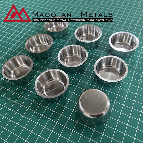
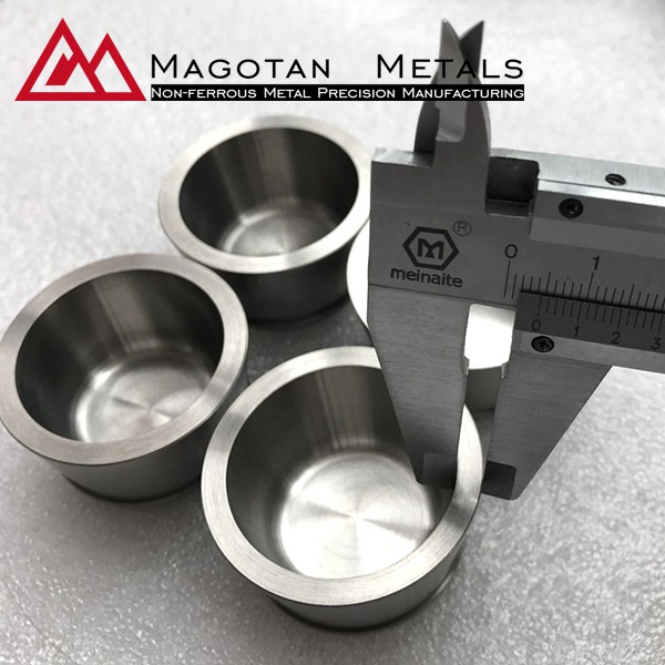
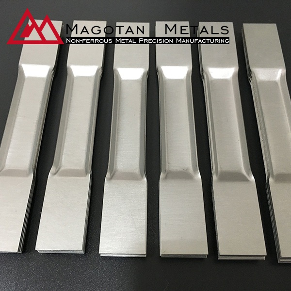
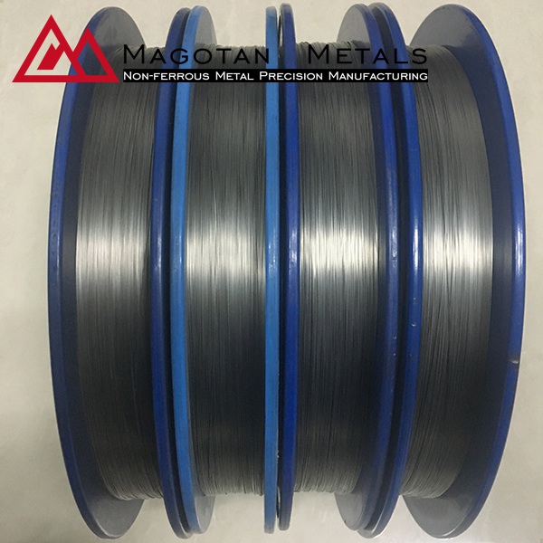
We take our customer’s custom metal fabrication designs and bring them to life.
Skip image slider
PVD Target Suppliers

Ultra-High Purity Tungsten Sputtering Targets (W Targets)

As leading PVD Target Suppliers, we provide 99.95% pure Tungsten Sputtering Targets for semiconductor, aerospace, and display industries, ensuring exceptional film uniformity and deposition rates.

  • Material Excellence
    99.95% purity with controlled oxygen/carbon content
    Fully dense microstructure (>99.5% T.D.)
  • Precision Engineering
    Custom geometries: planar, rotary, bonded targets up to 500mm diameter
    Surface roughness mirror finish available
  • Performance Optimized
    Sputtering yield 15-20% higher than industry average
    Thermal shock resistance up to 2000°C
Products Categories
Get A Free Quote
Contact Form

Engineered for Precision: Tungsten Sputter Target Solutions

Our Tungsten Sputtering Targets are vacuum hot-pressed using proprietary HIP technology, achieving superior grain structure uniformity (<50μm grain size). The targets feature:

  • Low Particulate Generation – Special edge treatment reduces arcing
  • Thermal Stability – Withstand 2000°C+ operating temperatures
  • Bonding Options – Indium/Elastomer bonding for improved heat dissipation
  • Ideal for DC/RF sputtering systems, these Tungsten Sputtering Targets demonstrate
  • 30% longer service life vs. industry average• ≤3% thickness uniformity across entire surface

Tungsten Target Physical Parameters

Parameter Standard Spec
Purity 99.95%
Density ≥18.9 g/cm³
Dimensions Ø50-300mm
Thickness 3-20mm
Orientation Random

As specialized Sputter Target manufacturers waht we deliver

  • Turnkey Service – From alloy design to post-sputtering analysis
  • Traceability – Full material genealogy reports with Lot ID tracking
  • Technical Support – 24/7 process optimization consulting

Tungsten Target Applications

Critical Thin Film Solutions

  • SemiconductorGate
    electrodes in 3nm/5nm nodes
    Barrier layers for Cu interconnects
  • Aerospace
    Thermal protection coatings for re-entry vehicles
    X-ray collimators in satellite systems
  • Flat Panel Displays
    TFT-LCD bus lines
    OLED encapsulation layers

Ultra-High Purity Tungsten Sputtering Target FAQ

Q1: What are the main applications of your ultra-high purity tungsten sputtering targets?
A1: Mainly used in high-tech fields needing critical thin film solutions: 1) Semiconductor: 3nm/5nm node gate electrodes, Cu interconnect barrier layers; 2) Aerospace: Re-entry vehicle thermal protection coatings, satellite X-ray collimators; 3) Flat Panel Displays: TFT-LCD bus lines, OLED encapsulation layers.
Q2: What is the purity of your tungsten sputtering targets and their material advantages?
A2: Purity 99.95% with strictly controlled O/C content. Material advantages: 1) Full density microstructure (>99.5% T.D.); 2) Uniform grain structure (<50μm) via proprietary HIP technology; 3) Low particulate generation for high-quality films.
Q3: What performance advantages do your tungsten sputtering targets have over industry averages?
A3: 3 key advantages: 1) 15-20% higher sputtering yield; 2) 30% longer service life; 3) ≤3% surface thickness uniformity. Also, thermal shock resistance up to 2000°C+.
Q4: Do you provide customized tungsten sputtering targets? 
A4: Yes. Customizable options: 1) Geometries: Planar/rotary/bonded (max φ500mm); 2) Dimensions: Standard φ50-300mm, thickness 3-20mm (other sizes available); 3) Surface finish: Mirror finish; 4) Bonding: Indium/Elastomer (enhanced heat dissipation).
Q5: What are the key physical parameters of your tungsten sputtering targets?
A5: Key parameters: 1) Purity: 99.95%; 2) Density: ≥18.9 g/cm³; 3) Dimensions: φ50-300mm, thickness 3-20mm; 4) Grain size: <50μm; 5) Orientation: Random; 6) Microstructure density: >99.5% T.D.
Q6: What manufacturing processes are used, and how is quality ensured?
A6: Manufactured via vacuum hot-pressing with proprietary HIP technology, ensuring uniform grains and full density. Special edge treatment reduces arcing and particulate generation, guaranteeing stable quality.
Q7: What value-added services do you provide as PVD target suppliers?
A7: 3 core services: 1) Turnkey Service: From alloy design to post-sputtering analysis; 2) Traceability: Full material genealogy reports with Lot ID tracking; 3) Technical Support: 24/7 process optimization consulting.
Q8: Are your tungsten sputtering targets compatible with common sputtering systems?
A8: Yes, compatible with DC/RF sputtering systems. Excellent thermal stability (2000°C+ resistance) and optimized bonding (facilitating heat dissipation) ensure stable performance.

Related Products

Related News & Industry Knowledge

Tungsten, a refractory metal with exceptional physical and chemical properties, has become an indispensable material in high-performance industrial applications. Its […]

Physical Vapor Deposition (PVD) has emerged as a cornerstone technology in advanced manufacturing, revolutionizing the performance and durability of components […]

The global semiconductor industry is undergoing a pivotal shift—accelerating adoption of wide-bandgap materials like gallium nitride (GaN) and silicon carbide […]

In high-end manufacturing sectors (semiconductors, optics, new energy, etc.), the selection of core film deposition technologies directly determines product performance […]

Scroll to Top

Get A Free Quote Now !

Contact Form